Computational Materials Modeling
Laboratory
The Computational Materials Modeling Laboratory conducts large-scale first-principles simulations based on density functional theory (DFT). Our research is carried out in close collaboration with experimental groups within the Department of Semiconductor Materials Engineering.
The Department’s activities are primarily focused on semiconductor applications in electronics and optoelectronics, including energy conversion, light emission, and photodetection. In this context, our work addresses the optical response of materials and nanostructures, as well as their electronic structure and its modification under external perturbations such as pressure, strain, electric fields, and magnetic fields.
We investigate systems of various dimensionalities (0D–3D), including bulk materials, low-dimensional structures, alloys (including digital alloys), van der Waals layered materials, crystal defects, systems with embedded magnetic moments, and perovskites.
Beyond electronic and optical properties, our simulations provide detailed insight into structural stability, elastic properties, and lattice dynamics — parameters that are essential for technological implementation and device applications.
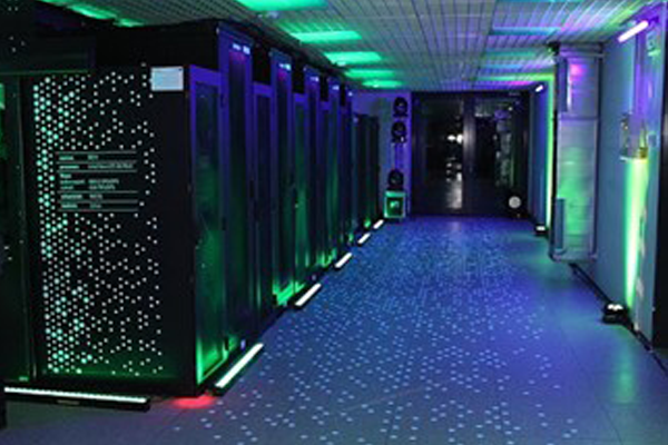
Our research relies on state-of-the-art high-performance computing (HPC) infrastructure. We primarily use the resources of the Wrocław Centre for Networking and Supercomputing (WCSS), including the BEM (photo) and LEM computing clusters. The main computational tools employed in our work are the widely recognized first-principles packages VASP (Vienna Ab initio Simulation Package) and Abinit.
In addition to research, we are actively involved in teaching activities focused on computational modeling, including materials science and atomistic modeling.
Contact
Prof. Robert Kudrawiec
E-mail: robert.kudrawiec@pwr.edu.pl
Tel. +48 713 204 280
Postal Address
Department of Semiconductor Materials Engineering
Wrocław University of Science and Technology
Wybrzeże Wyspiańskiego 27
50-370 Wrocław
Poland