Deep Level Transient Spectroscopy
Laboratory
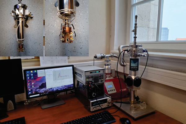
The Deep Level Transient Spectroscopy (DLTS) Laboratory is dedicated to advanced electrical characterization of semiconductor materials. DLTS is a highly sensitive experimental technique used to study electrically active defects in semiconductors. It determines fundamental defect parameters such as activation energy, capture cross-section, defect concentration, and depth profiles. These parameters serve as characteristic “fingerprints” for defect identification and analysis. DLTS measurements are typically performed on simple semiconductor devices such as Schottky diodes or p-n junctions, enabling investigation of defects located in the space charge (depletion) region. The technique offers extremely high sensitivity, allowing detection of defect concentrations as low as one part in 10¹² of the host atoms.
The DLTS laboratory is equipped with a modern measurement system that enables comprehensive studies of deep-level defects using both conventional and high-resolution techniques over a wide temperature range. It provides:
- electrical and electro-optical characterization in the temperature range 77 – 800 K,
- precise 2-point and 4-point measurements,
- I-V-T and C-V-T characterization,
- conventional DLTS and high-resolution Laplace DLTS,
- Impedance Spectroscopy (IS).
These capabilities enable quantitative defect identification, determination of fundamental physical parameters, and optimization of semiconductor materials and device structures.
Research activities include investigations of electrical properties and defect physics in a wide range of semiconductor materials, including:
- III–V compounds (e.g. GaAs, InGaAs, GaN, …);
- group IV materials (e.g., Si, SiC, …);
- highly mismatched alloys, such as dilute nitrides (GaAsN, InGaAsN, …), bismides (GaAsBi, InPBi), and borides (BGaAs, BGaInAs, …);
- transition metal mono- and dichalcogenides (e.g. MoS2, MoSe2, WS2, WSe2, ReSe2, InSe, SnSe, GeS, …)
- perovskite-based devices (e.g. solar cells, light-emitting diodes, …)
- other advanced semiconductor systems.
Contact
Prof. Robert Kudrawiec
E-mail: robert.kudrawiec@pwr.edu.pl
Tel. +48 713 204 280
Postal Address
Department of Semiconductor Materials Engineering
Wrocław University of Science and Technology
Wybrzeże Wyspiańskiego 27
50-370 Wrocław
Poland