Device prototyping/testing
Laboratory
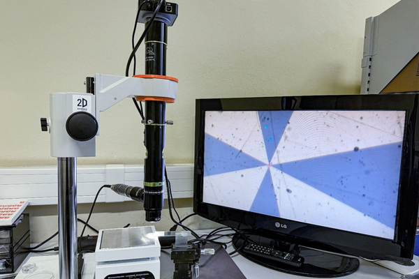
Device prototyping/testing focuses on the fabrication and characterization of electronic devices based on two-dimensional (2D) materials. The laboratory specializes in the transfer of mechanically exfoliated flakes onto pre-patterned substrates with electrical contacts, enabling rapid prototyping of functional structures. In addition, dedicated measurement setups are developed to perform electrical testing and performance evaluation of the fabricated devices.
M. Tamulewicz, J. Kutrowska-Girzycka, K. R. Gajewski, J. Serafińczuk, A. Sierakowski, J. N. Jadczak, L. Bryja, T. Gotszalk
Layer number dependence of the work function and optical properties of single and few layers MoS2: effect of substrate
Nanotechnology, vol. 30, nr 24, s. 1-8, 2019
M. Tamulewicz-Szwajkowska, S. J. Zelewski, J. Serafińczuk, R. Kudrawiec
Geometric progress in the thickness of exfoliated van der Waals crystals on the example of MoS2
AIP Advances, vol. 12, nr 2, s. 025328, 2022
Contact
Prof. Robert Kudrawiec
E-mail: robert.kudrawiec@pwr.edu.pl
Tel. +48 713 204 280
Postal Address
Department of Semiconductor Materials Engineering
Wrocław University of Science and Technology
Wybrzeże Wyspiańskiego 27
50-370 Wrocław
Poland