X-ray diffraction
Laboratory
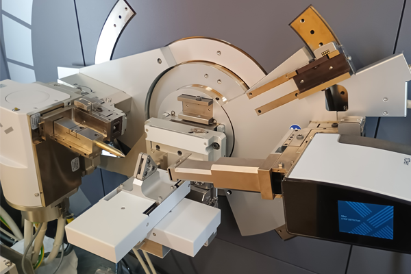
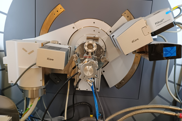
The X-ray Diffraction Laboratory at the Department of Semiconductor Materials Engineering is equipped with a state-of-the-art Empyrean X-ray diffractometer manufactured by Malvern Panalytical. This diffractometer enables measurements of a wide range of materials — from powders and bulk solids to thin films and epitaxial layers or structures. The instrument is equipped with Cu, Mo, and Ag X-ray tubes, allowing for flexible adaptation to different experimental needs. The diffractometer setup includes various sample stages, such as:
- a stage for powder measurements in Bragg–Brentano geometry,
- a stage dedicated to thin film measurements without height correction,
- and a five-axis sample stage for high-precision alignment.
Additionally, the laboratory is equipped with low- and high-temperature sample chambers enabling measurements within the temperature range from 12 K to 700 K, as well as diamond anvil cells allowing high-pressure studies up to 15 GPa. Such comprehensive equipment allows for a broad spectrum of material investigations, including the determination of the following structural parameters: Powder diffraction:
- phase identification,
- stress measurements (sin²ψ method),
- thin film analysis using grazing incidence diffraction (GIX)
- X-ray reflectometry (XRR),
- pole figure measurements.
High-resolution X-ray diffraction (HRXRD):
- rocking curve measurements,
- reciprocal space mapping (RSM),
- determination of composition and strain in epitaxial structures,
- dislocation density evaluation,
- analysis of the shape and size of quantum dots (QDs) in epitaxial layers.
Non-ambient measurements:
- high-pressure studies up to 15 GPa,
- low-temperature measurements in the range of 12 K to 300 K or 70 K to 300 K (liquid nitrogen),
- high-temperature measurements from room temperature (~298 K) up to ~700 K, performed either in air or under controlled gas atmospheres.
Contact
Prof. Robert Kudrawiec
E-mail: robert.kudrawiec@pwr.edu.pl
Tel. +48 713 204 280
Postal Address
Department of Semiconductor Materials Engineering
Wrocław University of Science and Technology
Wybrzeże Wyspiańskiego 27
50-370 Wrocław
Poland